PhysicsElectronics › Discrete semiconductor devices

Discrete semiconductor devices

Four components with four jobs. A transistor whose gate takes almost no steady current switches amps from a logic pin, a diode run backwards pins a supply rail steady, and two more turn light and magnetic field into numbers a circuit can read.

Builds on Current-voltage characteristics and Force on a moving charge.

IN THIS TOPIC

  • Read a MOSFET's drain characteristic, and use the threshold voltage to say whether the channel is open.
  • Explain how a logic-level gate voltage switches a load, and why the gate itself takes no steady current.
  • Use a zener diode and its series resistor to hold an output steady against a wandering supply.
  • Say what a photodiode and a Hall effect sensor each measure, and choose between a photodiode and an LDR.

COMMON MISCONCEPTION

Switching a heavy load needs a heavy current into the transistor's control terminal.

A gate that takes no current

A MOSFET has three terminals. The load current flows between the drain and the source, and the gate controls whether it flows at all. The gate sits on a thin insulating layer of oxide, out of contact with the silicon beneath, so it behaves as a very small capacitor rather than as a way in. Put a voltage on it and its field reaches through the oxide and draws carriers into a conducting channel underneath.

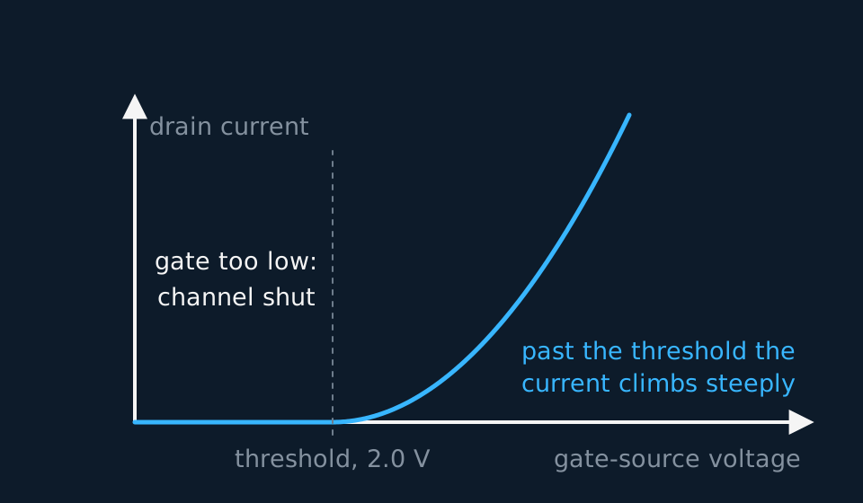
Nothing useful happens until the gate-source voltage passes the threshold voltage VTV_{T}. Below it no proper channel forms, so the drain current is negligible, a leakage far smaller than the current the device carries when it is on, for any drain voltage within the maker's rating. Driven past that rating any MOSFET breaks down and conducts, which is a failure rather than a mode of operation.

Past the threshold the channel opens and widens, and provided the drain voltage is large enough to keep the channel saturated, the drain current is approximately proportional to the square of the excess above threshold. Take that pair of statements as the model for the rest of this lesson: an idealised switch, off below threshold and square-law above it, working inside its ratings.

A MOSFET's drain current is negligible until the gate passes the threshold voltagegate-source voltagedrain currentthreshold, 2.0 Vgate too low:channel shutpast the threshold thecurrent climbs steeply
FIG. 1Drain current against gate-source voltage on the idealised square-law model. The current is negligible below the threshold at 2.0 V, drawn there as exactly zero, and past it a small extra gate voltage produces a large drain current.

WORKED EXAMPLE

One volt over, two volts over, three

The MOSFET drawn above has VTV_{T} = 2.0 V, and at VGSV_{GS} = 3.0 V it passes 0.10 A. Predict the drain current at 4.0 V and at 5.0 V, taking the square-law model to hold with the channel saturated.

The excess above threshold is 1.0 V, 2.0 V and 3.0 V in turn, and on the square law the current follows its square.

Doubling the excess quadruples the current, giving 4 × 0.10 = 0.40 A. Three times the excess gives nine times the current, 9 × 0.10 = 0.90 A, the top of the drawn curve.

That doubling test is the quick check on any drain characteristic. A straight line through those points would be the wrong shape entirely.

Switching a load

That shape of characteristic makes a superb switch. Wire the load in series with the drain and drive the gate from a logic output. At 0 V the channel is shut, the drain-source resistance is megohms, and the load sees microvolts. At a gate voltage comfortably past the threshold, 5 V on a logic-level device whose data sheet specifies its low on-resistance there, the channel is fully enhanced, its resistance falls to a fraction of an ohm, and almost the whole supply lands on the load. Reaching the threshold alone is not enough: the threshold is where conduction begins, and the guaranteed low resistance arrives at the higher gate voltage the data sheet names.
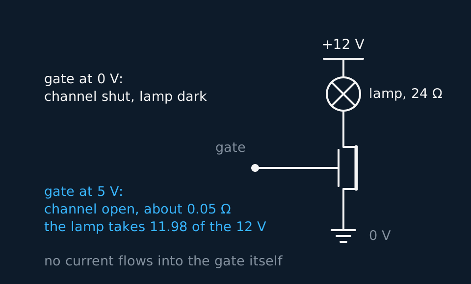
A MOSFET switching a lamp: the gate voltage decides whether the load sees the supply+12 Vlamp, 24 Ω0 Vgategate at 0 V:channel shut, lamp darkgate at 5 V:channel open, about 0.05 Ωthe lamp takes 11.98 of the 12 Vno current flows into the gate itself
FIG. 2A MOSFET switching a 24 Ω lamp across a 12 V supply. At 0 V on the gate the lamp is dark; at 5 V the channel is worth about 0.05 Ω and the lamp takes 11.98 of the 12 V.

Work the on state as a potential divider, modelling the lamp as a constant 24 Ω at its working temperature. Lamp and channel carry 12/24.05 = 0.499 A between them, the lamp keeps 11.98 V, and the MOSFET dissipates I2RI^{2}R = 0.012 W against nearly 6.0 W in the lamp. A component wasting a hundredth of a watt to control six of them needs no heat sink.

The gate is insulated, so only a negligible leakage current enters it once it is charged. A logic output has only to charge a gate capacitance of a nanofarad or two, which it does in microseconds, and in between it supplies almost nothing.

Holding a rail steady

Run an ordinary diode backwards and it blocks until the reverse voltage grows large enough to destroy it. A zener diode is built to break down gently at a chosen voltage VZV_{Z} and to survive the experience indefinitely, so long as its rated current and power are respected. Past breakdown its characteristic is nearly vertical, so the current through it can swing by tens of milliamps while its pd barely moves.

A component whose voltage stays almost constant is what a supply rail needs. So the zener goes across the load, reverse biased, with a series resistor between it and the raw supply. The load gets VZV_{Z}, everything left over is dropped across the resistor, and when the supply wanders it is the resistor's share that changes.

A zener regulator: the output holds near the breakdown voltage, while the zener stays in breakdown and within rating, and the series resistor drops the restinput, 9 V to 15 VR = 390 Ωzener, 5.1 Vloadoutput ≈ 5.1 V in breakdownthe resistor sets the current; the zener takes what the load leaves9.0 V in: 3.9 V across R, ≈5.1 V out12.0 V in: 6.9 V across R, ≈5.1 V out15.0 V in: 9.9 V across R, ≈5.1 V out
FIG. 3A 5.1 V zener regulating a load fed from a supply that wanders between 9 V and 15 V. The 390 Ω resistor drops 3.9 V, 6.9 V and 9.9 V in turn, and the output holds near 5.1 V, valid while the zener stays in breakdown and within its power rating. The zener's share is what the load leaves, IZ = IR − Iload, so it regulates only while that stays inside the valid current range.

The resistor sets the current, and the current is what the design turns on:

I=VS-VZRSI = \frac{V_{S} - V_{Z}}{R_{S}}NOT ON THE AQA DATA SHEET: LEARN IT

Too small a current and the diode never properly reaches breakdown. Too large and it overheats. In the figure the resistor carries 10.0 mA at 9 V in and 25.4 mA at 15 V in, and the zener carries whatever the load leaves.

GUIDED PRACTICE

Sharing the current

The regulator above runs from 12 V. Find the current in the 390 Ω resistor, then the current in the zener when the load draws 8.0 mA, and the power the zener dissipates.

Show the working

The resistor drops 12 − 5.1 = 6.9 V, so it carries 6.9/390 = 17.7 mA.

The load takes 8.0 mA of that, leaving 17.7 − 8.0 = 9.7 mA in the zener, and a power of 5.1 × 9.7 × 10−3 = 49 mW.

Ask the load for more than 17.7 mA and the zener current would have to run backwards, which it cannot. The output sags below 5.1 V and regulation is lost.

Light into current

A photodiode is a diode with a window, used reverse biased so that almost nothing flows in the dark. A photon absorbed in the depletion layer frees an electron-hole pair, and the strong field there sweeps the two apart before they can recombine. Every absorbed photon therefore adds to a small reverse current, the photocurrent, and doubling the illumination doubles the pairs freed each second.

A reverse-biased photodiode: the photocurrent is proportional to the illumination and almost independent of the pdreverse voltagephotocurrent20 μA: one unit40 μA: two units60 μA: three unitsdark currentflat: the light sets the current
FIG. 4Photocurrent against reverse voltage at three illuminations, 20 μA per unit of light. Each line is flat, so the pd across the diode hardly matters; the light sets the current. A dark current of 0.8 μA flows with no light at all.

Those flat lines carry two messages. Photocurrent is proportional to illumination, so a single constant, the responsivity, describes the device where a curved characteristic would have needed a whole calibration graph. That is not the same as needing no calibration at all. The constant itself still has to be found against a known source, and it depends on the wavelength of the light, differs from one device to the next and drifts with temperature, while the small dark current that flows with no light on the window has to be subtracted as well. Linearity makes the calibration short, not unnecessary.

The second message is that the current hardly depends on the applied pd, so the diode behaves as a current source. Read it by dropping its current across a resistor: 40 μA through 50 kΩ gives 2.0 V, and 60 μA gives 3.0 V.

Against a light-dependent resistor the photodiode wins on speed and on linearity. Carriers in an LDR take milliseconds to build up and longer to disperse, so it cannot follow anything flickering faster than a few hundred hertz, and its resistance is nowhere near proportional to the light. A photodiode responds in nanoseconds, which puts one at the end of every optical fibre. Where the light changes slowly, the cheaper LDR is fine.

Measuring a field, and noticing a magnet

Send a current along a thin slab of semiconductor and put a magnetic field through its face. Each moving carrier feels a force BQvBQv at right angles to both, so carriers pile up along one edge and leave the opposite edge short of them. The separated charge builds a field that opposes further pile-up, and matters settle once the two forces balance. What remains is a steady Hall voltage across the faces.

The Hall effect: a field across a current-carrying slab pushes charge to one face, and the voltage across the faces measures the field+ + + +− − − −positive carriers shown: polarity reverses for electronsfield into the pagecurrent inand outvoltage across the faces0.20 T reads 2.4 mV0.40 T reads 4.8 mVno field, no reading:so it senses proximity too
FIG. 5Current from left to right, field into the page, drawn for positive carriers, which pile onto the top face; for electron carriers the polarity across the faces reverses. The voltage doubles from 2.4 mV to 4.8 mV when the flux density doubles.

Hold the current constant and that voltage is proportional to the flux density, so the slab is a direct-reading field meter. A Hall probe is exactly that, calibrated. Its reading is largest when the field runs perpendicular to the slab's face, so a probe is rotated for a maximum before the number is taken. The sensor above gives 2.4 mV in 0.20 T and 4.8 mV in 0.40 T, a sensitivity of 12 mV per tesla.

INDEPENDENT PRACTICE

Counting the shaft round

That sensor is mounted beside a rotating shaft carrying one small magnet, which brings 0.35 T past the slab once per revolution. Find the peak output, and explain how the circuit measures the rotation rate.

Show the working

The sensitivity is 2.4/0.20 = 12 mV T−1, so 0.35 T gives 12 × 0.35 = 4.2 mV.

Away from the magnet the field is near zero and so is the output, so the sensor delivers one pulse per revolution. Counting pulses per second gives the rotation rate.

Proximity sensing is the same trick standing still. Bring a magnet close and the voltage appears, take it away and it vanishes, with no contacts to wear out.

ASSESSMENT FOCUS

  • Threshold answers want the word channel. Below VTV_{T} no channel exists, so the drain current is negligible at any drain voltage within the device's rating, and above it, in saturation, the current rises approximately with the square of the excess.
  • For a switching calculation put the channel resistance in series with the load and divide. Quote the load's pd, and the power lost in the MOSFET as I2RI^{2}R if the question asks.
  • The insulated gate is worth two marks whenever a MOSFET is compared with anything else. No steady gate current flows, so the driver supplies only the charge the gate capacitance needs to change state.
  • Zener answers begin with the resistor's drop, supply minus VZV_{Z}, then Ohm's law. The zener current is the resistor current minus the load current, and regulation holds only while that difference stays positive.
  • Write reverse biased and proportional to intensity into every photodiode answer. A comparison with an LDR is won on response time and on linearity, not on cost alone.

CHECK YOURSELF

A MOSFET with a threshold voltage of 2.0 V switches a 24 Ω lamp across a 12 V supply, and its channel resistance is 0.05 Ω with the gate at 5 V. State the drain current with the gate at 1.5 V. Find the lamp's pd and the power wasted in the MOSFET with the gate at 5 V. Explain how a logic output rated at 1 mA can drive it.

Show a hint

Below the threshold nothing flows. Above it, treat the open channel as a small resistance in series with the lamp.

Show the answer

At 1.5 V the gate is below the threshold, so no channel forms and the drain current is negligible, effectively zero beside the half-amp the lamp draws once the switch is on.

With the gate at 5 V the series resistance is 24.05 Ω, so the current is 12/24.05 = 0.499 A and the lamp holds 0.499 × 24 = 11.98 V.

The MOSFET dissipates I2RI^{2}R = 0.4992 × 0.05 = 0.012 W, against 6.0 W in the lamp.

The gate is insulated from the channel, so it draws no steady current. The logic output supplies only the brief charging current of the gate capacitance, well within 1 mA.

No channel below the threshold voltage, so the drain current is negligible; in saturation above it the drain current climbs roughly with the square of the excess.

A MOSFET gate is insulated, so it takes no steady current and a logic pin can switch amps.

A zener holds its breakdown voltage across the load while the series resistor drops whatever is left.

Photocurrent follows the light; the Hall voltage follows the flux density.

WORKBOOK

Printable practice for this topic: original exam-style questions with room to work, and a fully worked answer book. Free to use; please do not redistribute or sell.

17 questions on this topicAnswer them one at a time and mark yourself against the mark scheme.Practise this topic

Or read them with their mark schemes on the discrete semiconductor devices questions page.

6 flashcards on this topicDefinitions, off-sheet equations and a spot-the-error card, scheduled by spaced repetition in your browser.Revise with flashcards

CHECK YOUR PROGRESS

Rate how confident you feel with each objective for this lesson. Ratings are saved in this browser, on this device, unless you sign in.

  • Read a MOSFET's drain characteristic, and use the threshold voltage to say whether the channel is open.
  • Explain how a logic-level gate voltage switches a load, and why the gate itself takes no steady current.
  • Use a zener diode and its series resistor to hold an output steady against a wandering supply.
  • Say what a photodiode and a Hall effect sensor each measure, and choose between a photodiode and an LDR.

Open the full revision checklist to track your progress across the whole unit.